Hello everyone. I’m a beginner, so please help me.
Please tell me about EMI radiation noise.
I am considering creating a simple model of radiation noise by referring to Analysis and Modeling Method for EMI of Non-Isolated Converters (Part II) | Article | MPS
.
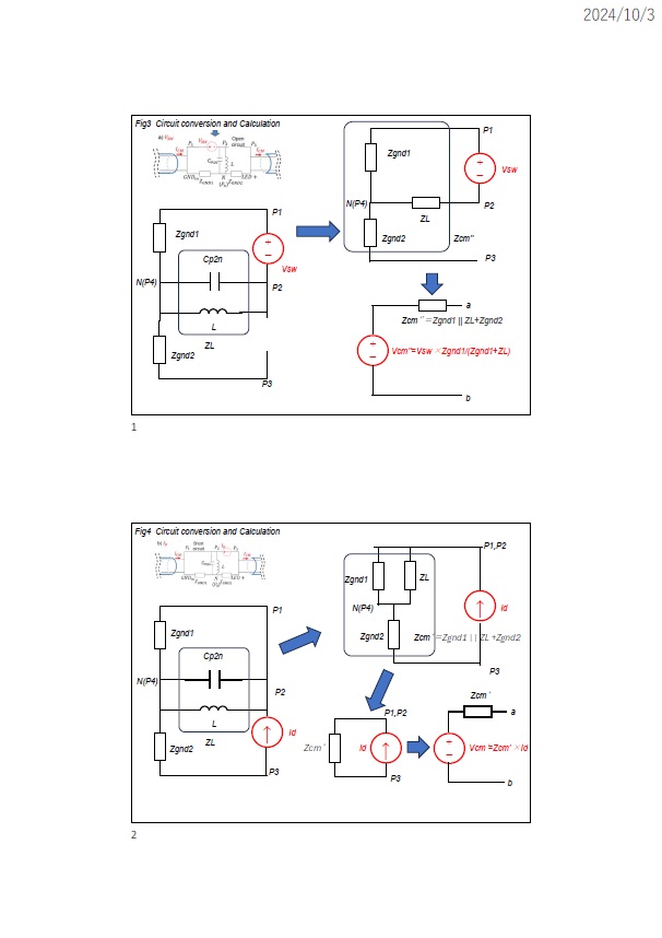
Figure 1 shows a power converter and an antenna. I understand that the left figure is the actual configuration and the right figure is the model, but which parts of the left figure do a and b in the right figure represent?
Also, I think that Vcm and Zcm in Figure 1 are Thevenin’s equivalent circuit, but please tell me how to calculate them from the actual values (voltage, current, inductance, capacitance, etc.) in Figures 3 and 4.
Hello, welcome to the MPS Forums!
On a general level Electromagnetic Interference (EMI) on a basic level is the electromagnetic energy that is emitted by electronic devices. There are many applications in which this emitted noise may cause interference with other electronic devices.
In regard to your questions on Figure 1:
- “a” in the right figure represents the high frequency noise sources of the converter. In practice, sources of high frequency EMI noise would be anywhere there are rapid changes in voltages like the switch node for example.
- “b” in the left figure represents the radiation path. In practice this would be dictated by the traces on the layout of a converter or any wiring that may inadvertently act as antennas where EMI noise may be radiated.
To address your questions on Vcm (Common Mode Voltage, which is the noise voltage driving radiated EMI through antenna) & Zcm (Common Mode Impedance, which is the impedance of the system that defines where the common mode current flows through the traces or wires acting as antennas radiating EMI):
- To calculate Vcm, this can be estimated by looking at the switching voltage waveform. If this is not available, you would need to calculate the average switching voltage of your converter. This calculation would differ depending on converter topology.
- To calculate Zcm, you would need to identify any parasitic capacitances and inductances in your system. So Zcm_L = Ljw for inductors and Zcm_C = 1/(Cjw) for capacitors where w = 2πF, where F = switching frequency of your converter.
I know that was a lot of information to take in at once. If you have any more questions, please reach back.
Best,
Krishan
Dear Krishan.
This is Matsukawa.
Thank you for your detailed reply.
Your reply said that Vm can be calculated or measured.
If calculating, does that mean using the voltage waveform of P3-Poutgnd at the bottom of Figure 2?
For example, can I calculate Vm by inputting Zgnd1 and Zgnd2 as shown in the bottom of Figure 2 using a SPICE simulator, setting the parasitic capacitance and parasitic inductance of each component and wiring, and running a simulation?
Correct, you may use the waveform of P3-Poutgnd at the bottom of Figure 2 for calculating and measuring Vcm. If you did simulate this and find the current going through any parasitic Zm, you would surely get your Vcm. The same logic may be applied in terms of actual measurements.
Hopefully this helped you,
Krishan
Dear Krishan.
This is Matsukawa.
Thank you for your detailed reply.
I now understand a little bit about how to simulate Vm.
I have an additional question.
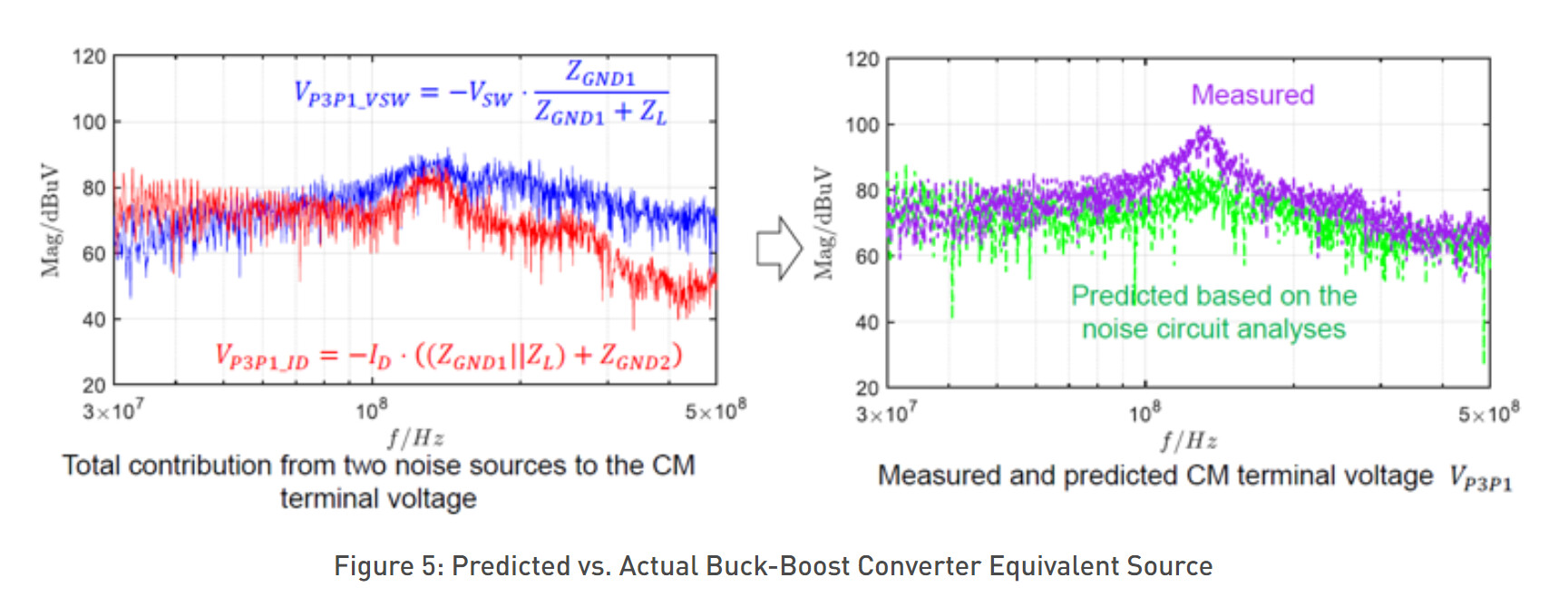
It is about Figure 5.
Vp3p1_VSW and Vp3p1_Id are listed in the frequency spectrum on the left side of Figure 5.
I confirmed that there is a formula on the right side for how to calculate this.
Does this mean that Vsw is the equivalent circuit of the MOSFET in Figure 3, and Id is the equivalent circuit of the diode?
For example, if I measure the time series data of Vsw and Id in a SPICE simulation and then perform FFT analysis on it, can I obtain the predicted noise data .
right side of Figure 5 by overlaying Vsw, Id and Vcm using a formula for each?
Correct, Vsw as seen in Figure 5 is the same as denoted in the equivalent circuit of the FET as seen in Figure 3. The same logic can be applied to Id as being the diode current in this case.
You should be able to obtain similar noise data in terms of getting the time series data for Vsw and Id via some SPICE simulation and performing the FFT.
Feel free to compare your calculations with your simulation and overlay them for accuracy purposes. This should also give you a range of where the actual measured data will vary. In this way you can account for this noise variance to your design.
Best,
Krishan
Dear Krishan.
This is Matsukawa.
Thank you for your detailed reply.
(1) I have an additional question about Figure 5.
The FFT calculation result on the right side of Figure 5 appears to show the average of
Vp3p1_VSW and Vp3p1_Id, but is this understanding correct?
(2) I have a question about Zcm.
How can I calculate Zcm? From Figures 3 and 4, it seems like Zcm = Zgnd2 + (Zgnd1 || Zl), but is
that correct?
This is a basic question, so I would appreciate your help.
Hello again,
To answer your next series of questions regarding the analysis and modelling for EMI in non-isolated converters:
-
Figure 5 shows the distributed noise calculated (right) and measured (left) in dBuV across 30MHz to 500MHz. The purpose of Figure 5 is to illustrate the accuracy of estimating the EMI of Vsw and Id by calculating them. So, it is more of an approximation of Vp3p1_VSW and Vp3p1_Id than an average.
-
Correct. Zcm for Id is Zcm = (Zgnd1 || Zl) + Zgnd2. This is further supported by the following image as seen in Figure 5 as outlined in the formula in red text using an Ohm’s Law approach:
Conversely, Zcm for Vsw is denoted as the impedance in blue using a voltage dividing approach.
Hope this helped,
Krishan
Dear Krishan.
This is Matsukawa.
Thank you for your detailed reply.
(1)I have a little understanding of question 1.
Looking at the right side of Figure 5, we can see that Id has a large effect from 30 MHz to approximately 120 MHz. Vsw has a large effect from approximately 120 MHz to 500 MHz.
I understand that the approximate range can be seen from the left side of Figure 5, and that it is possible to confirm from the actual measured values whether Vsw and Id have a large effect at each frequency.
(2)I have also a little understanding of question 2.
I have attached a diagram of my own circuit conversion and calculations. Please let me know if there are any mistakes.
Hello again,
These are some good questions.
-
The calculated noise spectrum as seen on the left is confirmed with measured values as seen on the right in the entirety of Figure 5. The consensus between the two noise spectrum graphs indicates that the magnitude of noise that is created has the most impact at around 100MHz. If you are talking about another method to verify these two graphs in Figure 5, let us assume that we sourced two graphs from calculation and simulation. We would at least have an estimated impact and expected variance between both simulated and calculated when compared to actual measured noise.
-
I see no mistakes in the attached images and calculations that you have provided. Good work.
Best,
Krishan
1 Like
Dear Krishan.
This is Matsukawa.
Thank you for your detailed reply.
I understand this method.
Please let me know if there are any reference papers or literature on this method. From what I have researched, I feel that the technical information on this method is insufficient in Japanese papers and literature. IEEE papers and the like are available in Japanese libraries, so it is possible to research them.
Hello again Matsukawa,
I would be happy to refer some more reference material for your research. Based off of the things that we had discussed and talked about, the following links I will share with you address and expand on the subject matter that you had questions about and more:
- Analysis and Modeling Method for EMI of Non-Isolated Converters (Part I) | Article | MPS (monolithicpower.com)
- Using Filter Capacitors and Inductors to Suppress Radiated EMI | Article | MPS (monolithicpower.com)
- Measuring High-Frequency, Common-Mode Current, Voltage, and Impedance (Part I) | Article | MPS (monolithicpower.com)
- Measuring High-Frequency, Common-Mode Current, Voltage, and Impedance (Part II) | Article | MPS (monolithicpower.com)
- Measuring High-Frequency, Common-Mode Current, Voltage, and Impedance (Part III) | Article | MPS (monolithicpower.com)
- Optimizing EMI in Switching Regulators for Consumer and RF-Sensitive Applications | Article | MPS (monolithicpower.com)
- PCB design for low-EMI DC/DC converters | Article | MPS (monolithicpower.com)
I am sure there are more articles like this on the IEEE website. Maybe these articles will give you a basis on what to look for depending on what questions you have. And if you need any of them answered, please reach back.
Best,
Krishan